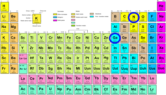
Welcome to the TSA Podcast! Today, we’re exploring a groundbreaking innovation in charging technology—Gallium Nitride (GaN) chargers.
Traditional chargers are often slow, bulky, and inefficient. GaN technology is changing that by offering faster charging speeds, compact designs perfect for travel, and superior energy efficiency. This advancement is reshaping how we power our devices, making charging more convenient and sustainable.
# What makes GaN chargers so revolutionary?
From their origins to their cutting-edge benefits, this episode covers everything you need to know. Whether you're a tech enthusiast or simply looking for a better charging solution, this is an episode you won’t want to miss.
Tune in now and upgrade your charging experience!
# History of Chargers:
Let’s start with a little history. Chargers, as we know them, have come a long way. For decades, silicon-based chargers were the industry standard. They powered everything from our phones to our laptops, but they had some serious limitations.
Bulky, heavy, and prone to overheating, these chargers were far from ideal, especially as our devices became more demanding. Silicon, the material at the heart of these chargers, could only go so far. Its inability to handle higher voltages efficiently or stay cool during intense use left a gap in the market—a gap that Gallium Nitride was poised to fill.
# What exactly is GaN?
At its core, GaN is a crystal-like semiconductor material. It was first used in LEDs and later found its way into other advanced technologies, including solar cells and satellites. But what makes GaN so special is its ability to handle electricity with unmatched efficiency. Unlike silicon, which has been pushed to its limits, GaN can switch electrical currents faster, manage higher voltages, and generate far less heat.

Here’s where things get really interesting. GaN transistors are tiny but mighty. These components can switch on and off up to 40 million times per second—four times faster than silicon transistors. This speed translates into incredible power efficiency. While traditional silicon chargers waste energy as heat, GaN chargers operate with over 95% efficiency. This means they stay cool, perform better, and last longer.
But the advantages don’t stop there. GaN’s efficiency allows for smaller designs. Imagine a charger capable of powering your smartphone, laptop, and tablet simultaneously—and small enough to fit in your pocket. That’s the magic of GaN. No more lugging around a tangle of cords and bulky adapters when one compact device can handle it all.
Take, for example, the Ugreen Nexode 300W GaN Desktop Charging Station. This powerhouse is capable of replacing multiple standalone chargers. With five ports and enough wattage to handle your most demanding devices, it’s a perfect illustration of how GaN technology is reshaping the market.
# Why is GaN such a leap forward?
To answer that, we need to talk about heat. Heat is the enemy of electronics. It reduces efficiency, damages components, and limits the power a device can handle. Silicon-based chargers are notorious for running hot, sometimes to the point of discomfort. GaN chargers, on the other hand, generate minimal heat, even under heavy use. This not only makes them safer but also prolongs their lifespan.
Efficiency isn’t just about performance—it’s about sustainability too. GaN chargers consume less energy and require fewer raw materials to manufacture, making them a greener choice. In a world increasingly focused on reducing waste and energy consumption, GaN is paving the way for a more sustainable future.
Now, let’s address some practical questions. What should you look for in a GaN charger? The first thing to consider is your power needs. If you’re only charging a smartphone or tablet, a 25W to 65W charger will do the trick. But if you’re powering a laptop or multiple devices, you’ll need something closer to 100W or more. Port types are another consideration. Most modern chargers feature USB-C, but if you still have devices that require USB-A, look for a charger with multiple port options.
Looking ahead, the future of GaN technology is brighter than ever. Over the next decade, we’ll likely see GaN chargers become the standard for everything from smartphones to electric vehicles. Their compact size and high efficiency make them ideal for cutting-edge applications, from portable charging solutions to EV fast-charging stations.
# Why should you care about GaN?
Because it’s not just a better charger—it’s a glimpse into the future of technology. In a world where we rely on devices more than ever, having a reliable, efficient, and sustainable way to power them isn’t just convenient—it’s essential.
As we wrap up, think about your current chargers. Are they meeting your needs, or are they holding you back? Maybe it’s time to upgrade to GaN and experience the difference for yourself.
Thank you for tuning into the TSA Podcast. Stay curious, stay connected, and as always, stay charged! See you next time.
Listen to the podcast :


